Physical Vapor Deposition (PVD), also known as Physical Vapor Transport (PVT), is a process used to produce coatings of metal circuits placed on thin-film-transistors used in displays. As you can assume from the use of the word ‘deposition’, PVD coating process is similar to that of snow falling and condensing into a single layer. In contrast to Chemical Vapor Deposition (CVD) that uses chemicals, PVD uses different physical mechanisms such as heat or collisional impact.
Physical Vapor Deposition is a process that coats TFT substrates with a thin, metallic layer used in an electric circuit that electrons move through. After coating formation, a photolithography method takes place for fabricating thin films. Sputtering and evaporation are the two most common types of PVD processes.
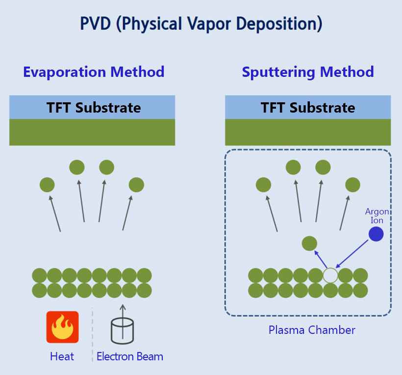
Evaporation method uses heat or an electron beam to coat on the TFT substrate. The material to be deposited as a film is converted into vapor by either applying heat to the source material in the vacuum chamber or bombarding material with an electron beam to evaporate and coat the substrate.
Sputtering, in physics, means small parts of a solid material are ejected from its surface because of the collision by energetic particles of a plasma or gas. Therefore, a sputtering method is a process that coats a TFT substrate using atoms that fell off of the original source material after being bombarded with an ionized gas molecule. Once plasma is generated by inserting argon into the vacuum chamber, argon ions are created to collide with the material used for coating. High energy particles such as argon ions have greater energy levels than that of the deposition material, and this is why the material disintegrates and sticks into the TFT substrate.