When coating thin layers on top of display substrates, chemical vapor deposition (CVD) is one of the methods used. As the name suggests, it refers to the process of using reactive gas to chemically deposit a thin film on the surface of a substrate.
Simply put, gas with thermal/plasma* energy creates chemical properties suited for stacking thin coatings on top of substrates.
* An electrically charged gas
With uniformly applied thickness and high purity as key advantages, chemical vapor deposition is a widely used thin film deposition method. The process easily coats on surfaces that traditional techniques (ex: solid/liquid deposition) cannot. In the display industry, chemical vapor deposition is used for depositing amorphous silicon (a-Si) layer on Low-Temperature PolySilicon (LTPS) or stacking insulator and buffer layers during Thin Film Transistor (TFT) manufacturing.
Plasma Enhanced Chemical Vapor Deposition (PECVD), Atmospheric Pressure Chemical Vapor Deposition (APCVD), Low Pressure Chemical Vapor Deposition (LPCVD) and High-Density Plasma Chemical Vapor Deposition (HDPCVD) are some of the many variations of chemical vapor deposition process based on different operating conditions such as type of activation energy initiation, reaction temperature, deposit materials, and level of pressure in the vacuum chamber.
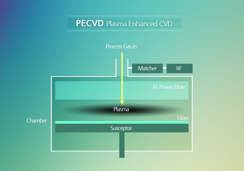
Plasma Enhanced Chemical Vapor Deposition (PECVD) is the most common coating method that heats gas in the vacuum chamber to create plasma. Think of plasma as a superheated gas with mixed positively charged particles (ions) and negatively charged particles (electrons).

Plasma Enhanced Chemical Vapor Deposition (PECVD) process is as follows: First we process reactant gas into the vacuum chamber, where it is heated by high voltage applied vertically to form plasma. A mixture of ions created by this plasma energy becomes reactive and coats thinly on the substrate prepared. After the deposition process, the remaining ions are discharged from the vacuum chamber as gas.


