Exposure (as in a material exposed to light) is part of the photolithography process used to produce a thin film transistor (TFT) that serves as the switch for a pixel in a display. The core mechanism of exposure is similar to that of photography, where the camera shutter opens to let external light in so that chemical changes are induced on the film to create an image.
Creating a microcircuit for a TFT requires a repeated process of depositing the material used for the circuit on a substrate and removing non-circuit areas. To do this, a photoresist (PR) is applied on top of the deposited material, and a mask designed with a circuit pattern is placed over the PR-coated material. Then, the exposure system is used to cast light for the PR to create the pattern of the mask.
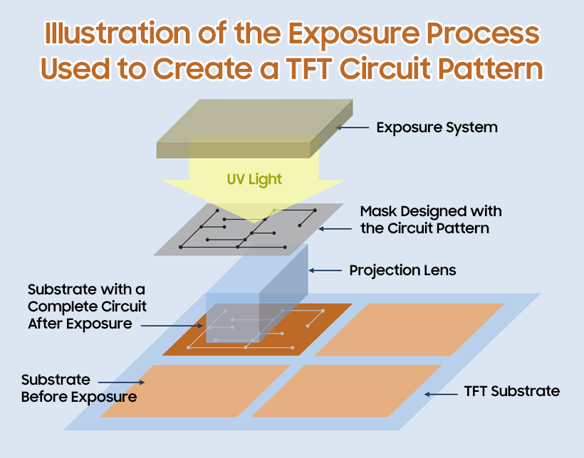
There are two types of exposure systems: a stepper and a scanner. Like how a camera takes a photo, a stepper casts light on the target area; a scanner uses light that follows a desired pattern to create it, similar to how a document scanner works.
As the circuit patterns required for display TFTs are measured in micrometers (㎛), UV light with a short wavelength is used as the light source in order to enhance the precision of the patterns. After the completion of the exposure process, properties of the PR change due to its exposure to light. Next, the development process removes unnecessary PR, leaving only the parts with desired patterns. Finally, through the etching process, substrates are patterned into circuits and the remaining PR is dissolved and eliminated.