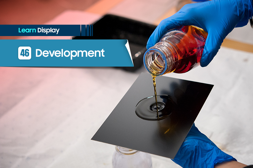
“Development” during the photolithography process for displays and semiconductors is similar to how photos are developed.
During the photolithography process, once we identify areas exposed to light vs. those that didn’t for photoresist (PR) coated materials, a solvent (developer) is used to remove unwanted parts: This is the development process.
In essence, the development process is about generating the desired colors and forms by placing a PR material (with parts exposed to light vs. parts with no light exposure) into developing agents such as alkaline.
A photoresist can be classified into positive and negative photoresist depending on the response to light.
With the positive photoresist, parts that are exposed to light change their chemical structure that makes it easily dissolved by the developer; when the developer is applied, parts that are exposed to light are eliminated.
Negative photoresist is when the parts exposed to light harden and the parts that are not exposed are removed with the developer.
The final outcome is determined by various factors such as prebake/developer/development temperature and exposure/development time.
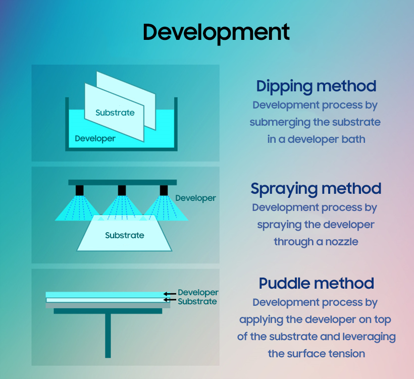
Developer solution is applied in three main approaches: ① Spray development uses a nozzle to distribute the developer, ② Puddle development leverages surface tension to dispense the developer solution onto the substrate, and ③ Dip development is when you dunk the substrate into a developer bath.