
Life at Samsung Display is a bimonthly introduction of exceptionally talented employees at different campuses around the world.
Tell us about yourself.
I'm a Principal Engineer at Samsung Display and a father of two children at the same time. It's important to work hard at work, but these days I also place time spent with my family as top priority. I am proud to have been a part of the team that developed the world's first publicly available flexible display at Samsung. I personally have experienced various flexible display development stages - from research up to mass production. Currently, I am doing a project that develops advanced foldable display module technologies in the Foldable Display Development Team.
Tell us more about your life before joining Samsung Display.
As an undergraduate, I studied electrical engineering at Korea University and semiconductor physics and fabrication processes as a graduate student at Seoul National University. When I was in graduate school, we were hit with the news about the global financial crisis. Back then, I was told that many manufacturing industries would not be able to grow further and some businesses would fall during the crisis. On the other hand, the display industry made significant progress with converting CRT to a thinner panel display, LCDs. I saw another future possibility converting from a flat panel to a flexible/foldable/rollable/stretchable panel and that came across as promising to me as a job applicant. Samsung Display was the best option among several display companies, because Samsung was a leading company in the LCD market and had mass produced the world's first AMOLEDs. That’s how I joined Samsung Display.
You were a recipient of the prestigious Samsung Display Scholarship. What was it like to study in the US?
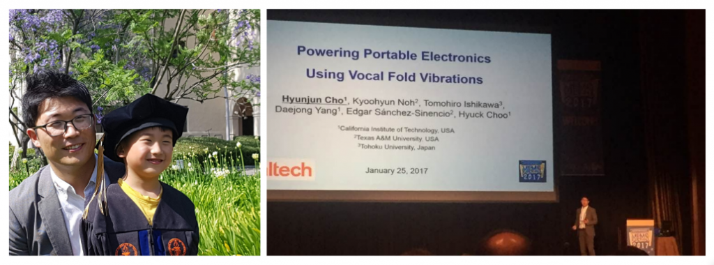
I was working on flexible display technology at Samsung Display when it occurred to me that I would like to further pursue my studies as a postgraduate student. Samsung Display has great education programs including academic support, language education, and career development programs. Luckily, I had a chance to study in the US for my doctoral degree as a recipient of the Samsung Display Scholarship that supported my Ph.D. studies for 5 years. I studied at California Institute of Technology (Caltech) and worked on ‘Wearable Devices: 1. Energy Harvesting using piezoelectric transducers and 2. Optical sensors using Raman spectroscopy (doi:10.7907/ZN7F-ZF71)’. During my time in the US, I participated in different academic conferences and even won the IEEE* MEMS** award. Studying in the United States was a great opportunity to foster a global mindset and harness a broader perspective in approaching work ethics and diversity. In my free time, I enjoyed traveling to places like Boston and Yellowstone National Park.
*The Institute of Electrical and Electronics Engineers: The world's largest technical professional organization for the advancement of technology
**Micro Electro Mechanical Systems
What is your daily responsibilities at Samsung Display?
My team is the Foldable Display Development Team in the Mobile Display Department. With a desire to make better displays, we develop the core technology of foldable modules and ensure reliability to stability of mechanical properties. Recently, our team developed an advanced material for foldable modules, which contributes to light weight.

For foldable displays, additional components need to be developed as the multi-layer structure such as the OLED panel gets more complicated. Each component has to show appropriate mechanical properties such as tensile modulus, flexure modulus, strain, creep, recovery, etc. Once mechanical properties meet the condition, the folding reliability is evaluated with stacked module structure. This reliability tests show the folding structure could be qualified under some sort of harsh environments that demonstrate hot humid or freezing weather, enormous number of folding repetitions, etc.
Due to the complicated nature of foldable displays, close cooperation with different teams (development team, quality control team, manufacturing technology team, customer support team, etc) takes place during mass production processes. It’s truly a rewarding experience since we are creating unprecedented technology that gets commercialized - impacting thousands of people on a daily basis.
Development engineers need to keep up with fundamental technologies and to constantly question and solve problems. Unfortunately, problem solving and creative thinking skills needed to carry out projects aren’t usually generated via work routines. That’s why I try to read recently released articles/papers and study problem solving methods inspired by other projects.
Tell us more about your work environment
I am currently working at Cheonan Campus in South Korea.
Cheonan Campus is where the mobile LCD displays were mass produced and the World's first AMOLED displays were manufactured. There was also a flexible AMOLED pilot line. The new displays have been introduced in this campus and I am proud that I am a part of the history.
Looking back, what would be the advice you would give to your younger self?
“What you will do is not always correct, but you won't need to regret.”
