
Photolithography is a process used for manufacturing semiconductors and displays. Similar to photographic printing technology, photolithography uses light to create complex circuit patterns.
In displays, photolithography is used in the thin-film transistor (TFT) fabrication process. The TFT fabrication requires a repeated process of constructing the TFT layer on top of the substrate by depositing layers, etching, and then depositing another layer, etc. The process of stacking layers of materials in the patterns desired by using light is called photolithography.
Photolithography follows a process illustrated below:
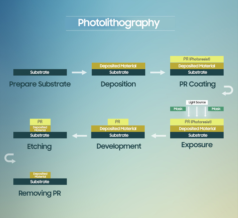
First, a layer of material required to manufacture a TFT is deposited evenly on top of a clean substrate. On top of this layer is applied a photoresist (PR), which reacts to exposure to light. Then, over the layer coated with the PR, a mask with the desired pattern is placed to be exposed to light so that the PR-coated layer is divided into parts exposed to light and parts that are not. The PR layer is classified into positive and negative method depending on the reaction to light.
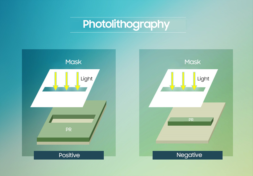
In the positive method, the chemical structure of the part of the photoresist exposed to light through a mask changes in a way that is conducive to dissolution when in contact with the developer. When the developer is applied, the parts exposed to light are removed.
On the contrary, the negative method hardens the part of the photoresist exposed to light and, parts that are not exposed to light are removed by using the developer.
The PR layer, now with only the desired pattern left, goes through the etching process so that the material deposited on parts not covered in the PR is removed. After the deposited material is formed into the desired pattern, the PR layer is removed so that only the deposited material in the desired pattern is left. Through the photolithography process, the stacked structure of a TFT is completed.