A pixel define layer (PDL) separates each sub-pixel from another in the emission material layer (EML) of an OLED display panel.
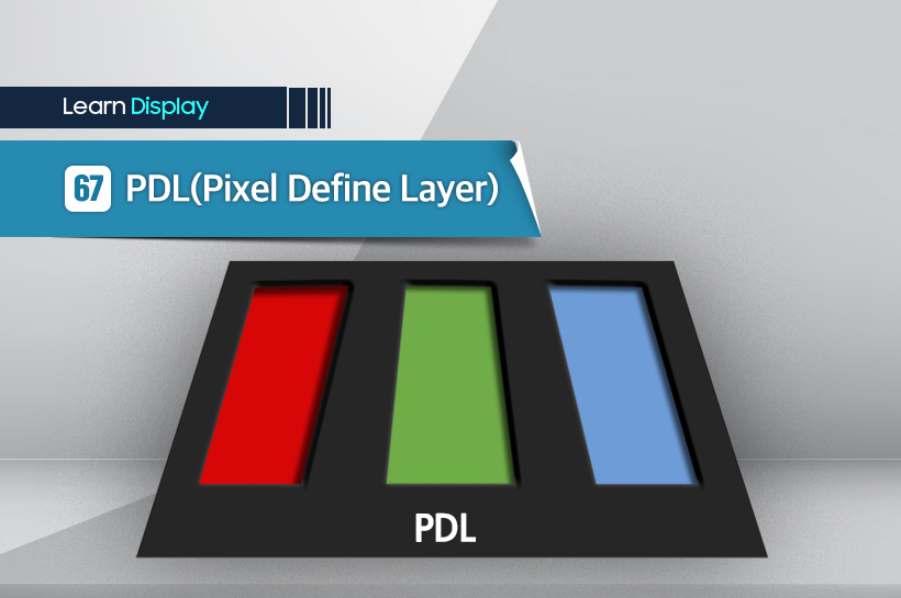
An OLED panel reproduces colors - Red, Green, Blue - using organic light-emitting materials, and each sub-pixel that emits RGB light is patterned through a process called evaporation. The pixel define layer (PDL) is deposited in areas that exclude the spots for the sub-pixels before the evaporation process is conducted for the organic light-emitting materials. In other words, the PDL is patterned in a way that leaves room for organic light-emitting materials (sub-pixels).
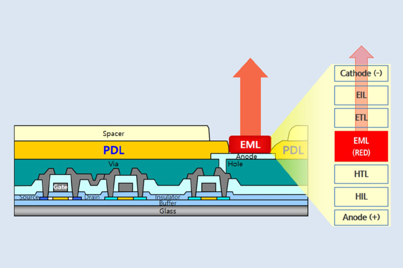
A pixel define layer uses polyimide (PI) and is patterned on the panel using the process called exposure (a photolithography process for TFT production). Once the areas for sub-pixels (not covered with the PDL) are defined, deposited organic materials come in contact with the anode below and emit light by using electrical signals. The pixel define layer prevents a short circuit in the electrodes of the sub-pixels and ensures that the organic materials do not spill over to the defined areas and blend.