
Sputtering is a type of physical vapor deposition (PVD) process used to form the metal layer for a display's thin-film transistor (TFT).
For easy movement of electrons, display TFT requires thin metal wiring; sputtering provides the basis of the wiring, while photolithography dissolves any areas not used for wiring.
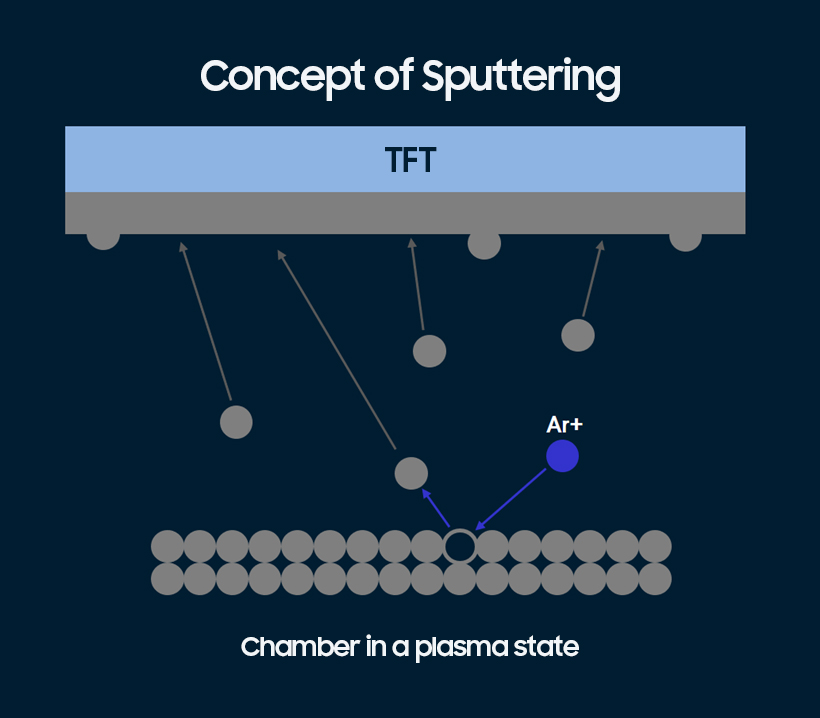
The first stage of sputtering begins inside a chamber by placing a TFT substrate and metal material meant for deposition. Low-pressure argon (Ar) gas is injected into the vacuum chamber, where the material to be deposited is exposed to a negative (-) charge to create an electric field between the TFT substrate (anode) and the material to be deposited (cathode), and the Ar gas that is exposed to this electric field becomes ionized to positive argon ions (Ar+), creating plasma inside the chamber.
The positive argon (Ar+) particles then collide with the deposited material (cathode). Particles of the emitted materials attach themselves to the TFT substrate (anode). This is how sputtering enables the thin deposition of metals on TFT substrates.