Depending on the direction of light emission, OLED displays can be divided into bottom emission and top emission types. The bottom emission display emits light toward the TFT substrate, while the top emission display emits light without the light going through the TFT substrate.
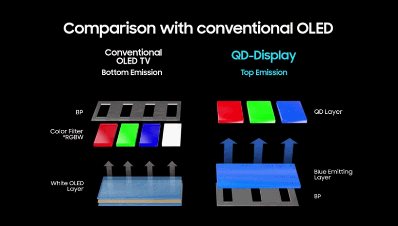
The bottom emission method was introduced during the early days of OLED development. At the time, the cathode (-) was made of metal, preventing the light emitted at the light source from passing through. For this reason, a transparent anode (+) material was used. However, when the light was emitted towards the direction of the anode, or in other words toward the direction of the substrate, some of the light was covered by the TFT surface and decreased the aperture ratio. This decrease had to be compensated for by increasing the density of the electric current in the same surface area of pixels, hampering the lifespan of the light-emitting material. This was particularly problematic for a mobile display where pixels are more densely arranged, making it hard to ensure high resolution.
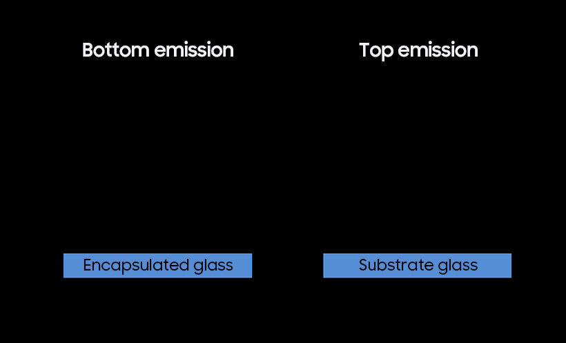
Top emission, on the other hand, emits light in the opposite direction of the substrate. This allows for circuits to be arranged freely on the substrate and minimizes the area where light is blocked, significantly improving the aperture ratio. As the aperture ratio is high, power usage and electric current density are lowered at the same brightness. This, in turn, extends the lifespan of the OLED light-emitting material and makes it easier to create high-resolution displays, regardless of the display size.