
Etching, by definition, means to sculpt forms through corrosion of the surface of a metal or glass. Etching in the context of displays refers to a process of eliminating undesired parts from a thin film transistor (TFT) to carve out the pattern of a circuit.
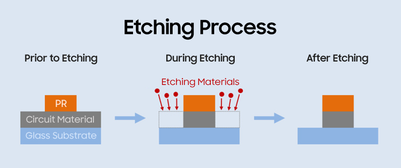
The exposure and development processes take place prior to the etching process, after which the photoresist (PR) remains only on the desired pattern for the circuit on the substrate. PR plays the role of a protective film for the desired pattern during etching. As seen in the illustration above, only layers coated with PR to be used as circuit remain while other parts are removed after the etching process.
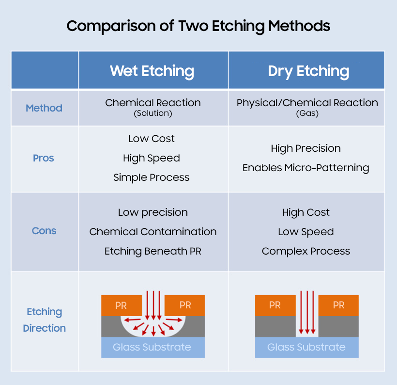
There are two types of etching methods: Wet and dry etching. Wet etching uses a solution to induce a chemical reaction to carve out a pattern, whereas dry etching removes specific parts by using reactive gas and ions.
Wet etching, compared to its dry counterpart, is cheaper, faster, and simpler. However, it is less precise compared to the dry method and it carries the risk of contamination due to the use of chemical substances in the process. Dry etching is more suitable to create a microcircuit thanks to its ability to easily target specific parts for etching. However, it is expensive, complex, and slow to process.
Dry etching is often referred to as plasma etching. In this process, an etching gas is injected into the vacuum chamber where the substrate is placed, and then electrical energy is provided into the chamber to create plasma. Afterward, ions that gain high levels of kinetic energy from the ionized gas are accelerated by the electrodes on the substrate so that the atomic bond in the circuit material is broken, which enables etching. Dry etching is the preferred method used for the majority of microcircuit patterns required for high-resolution displays today.