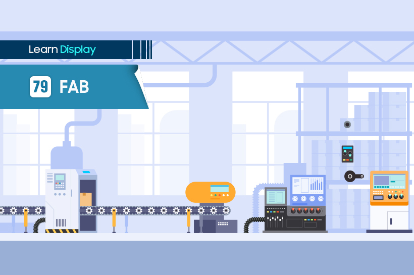
Display/semiconductor fabrication facility is commonly called a ‘fab’. In the fab, ultrafine fabrication processing for displays such as OLED and LCD takes place; every display panel undergoes Thin Film Transistor (TFT), evaporation (EV), and encapsulation (EN) fab processes.
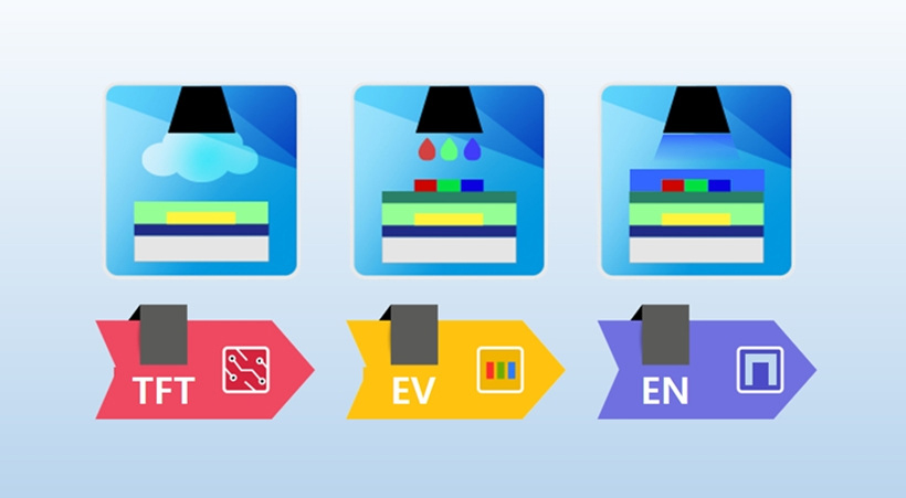
Fab processes such as TFT, EV, and EN all involve a vacuum chamber for chemical vapor deposition / physical vapor deposition / sputtering; due to chemical bonding within the vacuum chamber, it is crucial to ensure that every fab process has a structure that efficiently and sustainably carries out production.
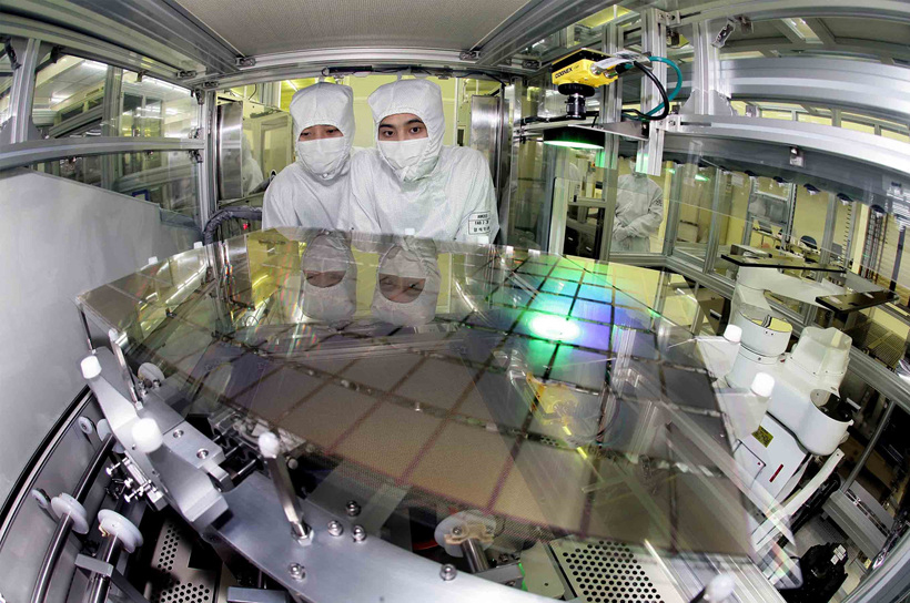
Fabs must be kept within narrow bands of temperature and humidity. It is also important to note that a single flake of dust/particle can be the cause of product defects, which is why fabs equip a separate space called a clean room that removes any contamination factors.